Radiometrix has been manufacturing radio modules for almost 40 years. In that time new designs have improved older ones, and technologies have changed. Some critical parts have even become obsolete. This has produced a family of legacy designs but Radiometrix does not just discontinue products and does not leave users options. Legacy modules can either still be manufactured (with some limitations and caveats) or technical support assistance can be provided to guide users towards more up to date (and often better, and cheaper) equivalents.
Our legacy product range includes the:
TX1, RX1, NRX1, NTX2, NRX2, BiM1 single channel crystal controlled narrowband modules
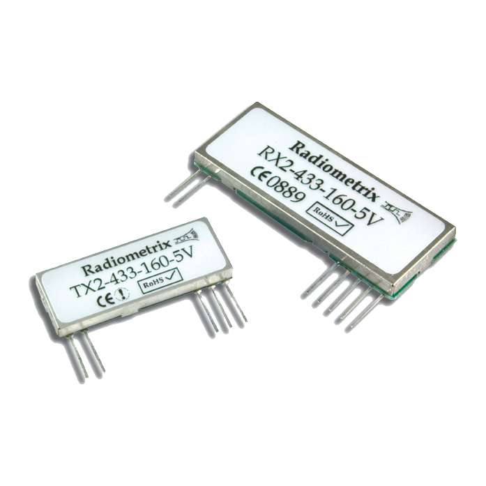
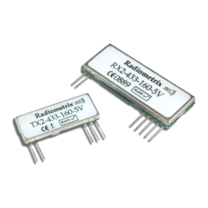
TX2, RX2, & BiM2 SAW based 433MHz radios. (Both supplanted by modern PLL based designs)
TX2A, RX2A, TX3A, RX3A, BiM2A, BiM3A, BiM2B, HVR2 (all with obsolescent part issues)
BHX2 (458MHz high power, transceiver superseded by SFX2).