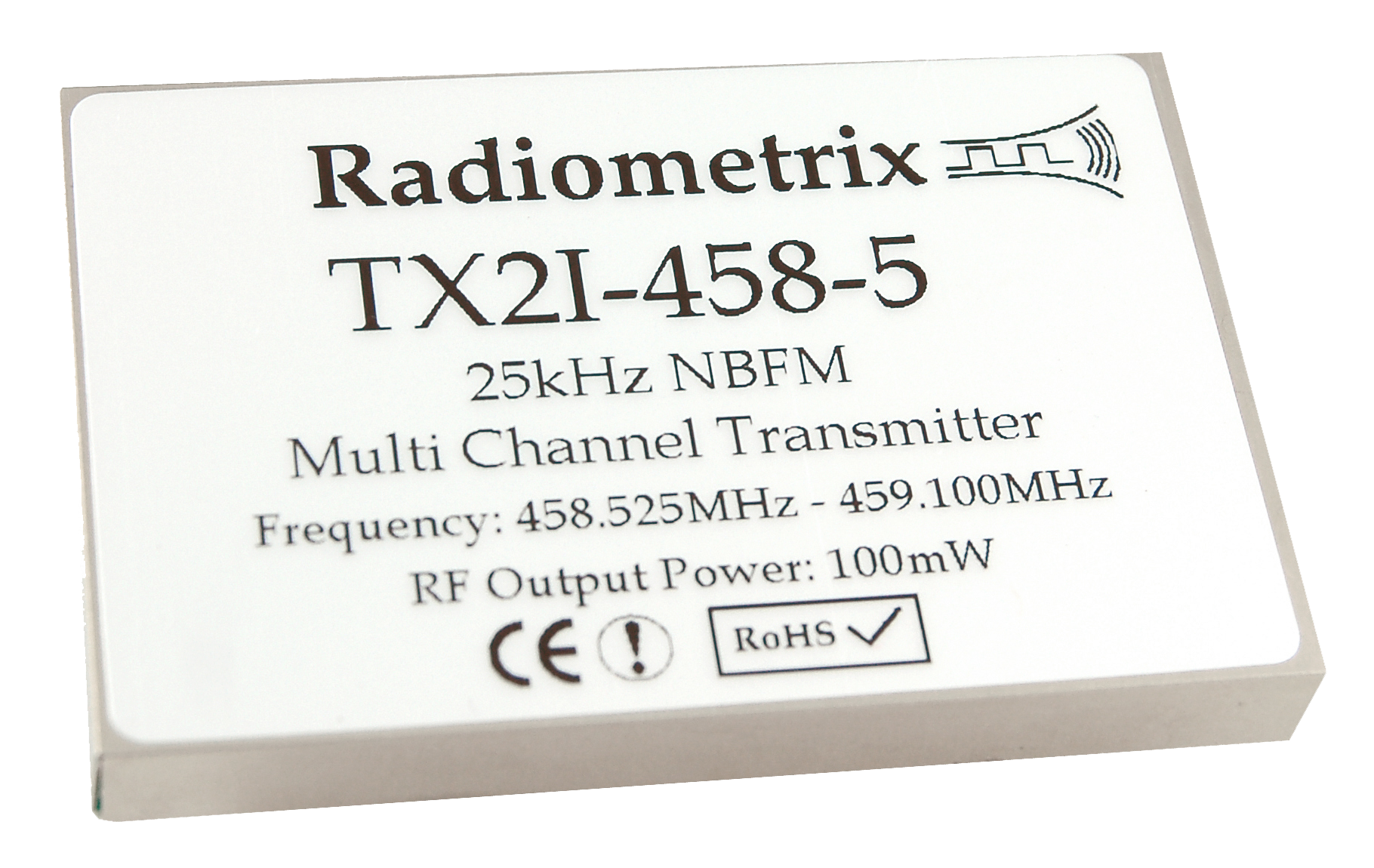
TX2M/RX2M
UHF Narrow Band FM Multi channel radio modules
The RX2M receiver and TX2M transmitter modules offer a low power, reliable data link in an industry-standard pin out and footprint. This makes the TX2M/RX2M pair ideally suited to those low power applications where existing wideband modules have insufficient range, or where multi-channel operation is needed.
Two versions are available, covering the 458.5-459.1MHz UK band (at 100mW) and the European 433.05-434.79MHz band.
Features
- 433MHz version conforms to EN 300 220-3 and EN 301 489-3 and 458MHz version to MPT 1329 (UK specs)
- Any custom band between 420MHz and 480MHz with 5MHz (AR0) frequency range
- High performance double superhet, 128 channel PLL synthesizer with TCXO
- Data rates up to 5 kbps for standard module
- Usable range over 1km
- Fully screened. Low profile
- Feature-rich interface (RSSI, noise squelch, analogue and digital baseband)
- Incorporate a 1200baud dumb modem
- Re-programmable via RS232 interface
- Low power requirements
Applications
- Handheld terminals
- EPOS equipment, barcode scanners
- Data loggers
- Industrial telemetry and telecommand
- In-building environmental monitoring and control
- High-end security and fire alarms
- Vehicle data up/download
Technical Summary
- Size: 59 x 38 x 7mm
- Operating frequency: 458.5-459.1MHz or 433.05-434.79MHz
- 23 channels in 458MHz band (128 channels max.)
- Transmit power: +20dBm (100mW) nominal
- Supply range: 4.5V - 16V
- Current consumption: 100mA transmit, 13mA receive
- Data bit rate: 5kbps max. (standard module)
- Receiver sensitivity: -118dBm (for 12dB SINAD)
Evaluation Platform: Narrow Band Evaluation Kit
Figure 3: TX2M Footprint (Top of the unit) view
Pin Description - TX2M
Pin | Name | Function |
Power: A | ||
1 | Vcc | +4.5V to 16V supply |
2 | Gnd | Ground |
RF: B | ||
1 | Gnd | RF ground |
2 | RF out | To antenna |
3 | Gnd | RF ground |
User: C | ||
1 | 0V | Ground |
2 | TXE | Transmitter enable. Low = ON, open = off. 4k7 pullup to raw Vcc |
3 | TXD | DC coupled input for 3-12V CMOS logic. Leave open if unused |
4 | AF in | AC coupled 1V pk-pk +/- 10% Analogue input |
5 | +4.4Vout | DC supply. 75mA max. drain. Only present when TXE is low |
6 | PGM | Serial programming/configuration input at RS232 level |
7 | 0V | Ground |
8 | P1 (mod TXD) | Parallel frequency select inputs. Inverted logic, 10k pullups to 4V |
9 | P2 (mod NC) | |
10 | P3 (mod TXH) |
Figure 4: RX2M Footprint (Top of the unit) view
Pin Description - RX2M
Pin
|
Name
|
Function
|
Power: A | ||
1 | Vcc | +4.5V to 16V supply |
2 | Gnd | Ground |
RF: B | ||
1 | Gnd | RF ground |
2 | RF in | To antenna |
3 | Gnd | RF ground |
User: C | ||
1 | RSSI | DC level between 0.5V and 2.5V. 60dB dynamic range |
2 | SQF | Noise operated carrier detect. Open collector. ON/low = no signal |
3 | AF out | 200mV pk-pk audio. DC coupled, approx 1V bias. Muted by squelch |
4 | RXD | Open collector output of data slicer. Need external pull-up |
5 | +4.4V out | DC supply. 75mA max. drain. Present if unit is powered |
6 | 0V | Ground |
7 | PGM | Serial programming/configuration input at RS232 level |
8 | P1 (mod NC) | Parallel frequency select inputs. Inverted logic, 10k pullups to 4V |
9 | P2 (mod RXD) | |
10 | P3 (mod C |
Note:
1. Internal AF Input gain is factory set for 1Vpk-pk to produce 3kHz peak deviation and minimum distortion. Analogue gain may be set for an input level of 50mV - 2V pk-pk. This cannot be done without appropriate test equipment. Contact factory for details
2. Carrier detect on RX2M mutes the AF and DATA outputs when RF input signal is <-123dBm. This can be factory disabled if required.
3. There are no pullups on the open collector outputs. External pull-up resistor should be used.
4. With 1200baud modem mode enabled, parallel selection of channel is unavailable as the P1-P3 lines are used for input/output operations.
TX2M and RX2M serial interface commands
2400 baud RS232. 8 bit data, no parity, 1 start bit, 1 or 2 stop bits, No flow control.
Transmit (pin 3 on DB9) and Signal Ground (pin 5 on DB9) should be connected to PGM and 0V pin.
SINGLE nnnnn | set value of N for single channel operation |
GOCHAN xx | serial select of channel xx (0 to 127) |
LOADMX xx | set highest permitted (serial selected) channel xx (others default to ch0) |
LOAD aa nnnnn | set value of N for channel aa (channels 0 to 15) |
LOADTB nnnnn | set value of N for channel 16 (channels 17 to 127 then in sequence) |
RVALUE rrrr | enter value for R register |
SETPAR | channel selected by 3 bit parallel input (0 to 7). Disable modem |
SETSER | channel selected by most recent 'gochan' operation |
SETMOD | enable internal modem. Frequency selected by most recent 'GOCHAN' or 'SINGLE' |
GOTEST | 250Hz test tone transmission |
<CR> | process entry (Carriage Return = 0D hex ) |
/ | clear all buffer |
xx = a channel number from 00 to 127
aa = a two digit channel number from 00 to 15
nnnnn = a synthesizer N register value, (up to 65535)
rrrr = the synthesizer R register value, (up to 16383)
, So R = 520
Channel number | 433MHz band | N value for TX | N value for RX | 458MHz band | N value for TX | N value for RX |
0
|
433.050 | /LOAD00 17322 | /LOAD00 16466 | 458.525 | /LOAD00 18341 | /LOAD00 17485 |
1
|
433.075 | /LOAD01 17323 | /LOAD01 16467 | 458.550 | /LOAD01 18342 | /LOAD01 17486 |
2
|
433.100 | /LOAD02 17324 | /LOAD02 16468 | 458.575 | /LOAD02 18343 | /LOAD02 17487 |
3
|
433.125 | /LOAD03 17325 | /LOAD03 16469 | 458.600 | /LOAD03 18344 | /LOAD03 17488 |
4
|
433.150 | /LOAD04 17326 | /LOAD04 16470 | 458.625 | /LOAD04 18345 | /LOAD04 17489 |
5
|
733.175 | /LOAD05 17327 | /LOAD05 16471 | 458.650 | /LOAD05 18346 | /LOAD05 17490 |
6
|
433.200 | /LOAD06 17328 | /LOAD06 16472 | 458.675 | /LOAD06 18347 | /LOAD06 17491 |
7
|
433.225 | /LOAD07 17329 | /LOAD07 16473 | 458.700 | /LOAD07 18348 | /LOAD07 17492 |
8
|
433.250 | /LOAD08 17330 | /LOAD08 16474 | 458.725 | /LOAD08 18349 | /LOAD08 17493 |
9
|
433.275 | /LOAD09 17331 | /LOAD09 16475 | 458.750 | /LOAD09 18350 | /LOAD09 17494 |
10
|
433.300 | /LOAD10 17332 | /LOAD10 16476 | 458.775 | /LOAD10 18351 | /LOAD10 17495 |
11
|
433.325 | /LOAD11 17333 | /LOAD11 16477 | 458.800 | /LOAD11 18352 | /LOAD11 17496 |
12
|
433.350 | /LOAD12 17334 | /LOAD12 16478 | 458.825 | /LOAD12 18353 | /LOAD12 17497 |
13
|
433.375 | /LOAD13 17335 | /LOAD13 16479 | 458.850 | /LOAD13 18354 | /LOAD13 17498 |
14
|
433.400 | /LOAD14 17336 | /LOAD14 16480 | 458.875 | /LOAD14 18355 | /LOAD14 17499 |
15
|
433.425 | /LOAD15 17337 | /LOAD15 16481 | 458.900 | /LOAD15 18356 | /LOAD15 17500 |
16
|
433.450 | /LOADTB 17338 | /LOADTB 16482 | 458.925 | /LOADTB 18357 | /LOADTB 17501 |
F max
|
434.775 | /LOADMX 69 | /LOADMX 69 | 459.100 | /LOADMX 23 | /LOADMX |
Please observe the following ERC/REC 70-03 (April 2004) Annex 1 recommendation when using the Non-specific Short Range Device (SRD) band for Telemetry, Telecommand, Alarms, Data in general and other similar applications.
Frequency Band | ERP | Duty Cycle | Channel spacing |
E (433.050 - 434.790MHz) | 10mW | <10% | No spacing |
E1 (433.050 - 434.790MHz) | 1mW | <100% | No spacing |
E2 (434.040 - 434.790MHz) | 10mW | <100% | <25kH |
Note: Audio and voice signals should be avoided in the band 433.050MHz - 434.790MHzPower density limited to -13dBm/10 kHz for wideband channels with a bandwidth greater than 250 kHz
Figure 5: Serial configuration of TX2I-458-5 transmitter using HyperTerminal
Figure 6: Maximum allowed and programmable channels
Notes:
1. A pause of at least 50ms must be allowed between command strings (EEPROM programming time) SINGLE mode does not store the N value in EEPROM. Therefore the unit is inoperative after a power down until either another valid SINGLE command is received, or mode is changed by a GOCHAN, SETPAR or SETSER command. SINGLE mode is intended for frequency agile applications.
2. /SETPAR command should be issued at the end of channel programming to put the module back into parallel frequency select mode
3. In 458MHz band, channel 12 (458.825MHz) and channel 15 (458.900MHz) are allocated specifically for fixed alarm and radio keys/vehicle paging applications respectively and should not be used for general purpose applications.
Pin description of TX2M/RX2M with Modem mode selected
The 'modem' mentioned is a 1200 baud RS232 semi-intelligent unit (Transmit keyed when valid serial data is present, so no separate TX control needed. Coding in the datastream also permits the receiver to ignore noise and only output valid serial data).
Pin Description - TX2M
Pin
|
Name
|
Function
|
1 | 0V | Ground |
2 | TXE | Must be tied to 0V |
3 | N/C | |
4 | N/C | |
5 | +4.4Vout | DC supply. 75mA maximum drain. Only present when TXE is low |
6 | PGM | Serial programming/configuration input at RS232 level |
7 | 0V | Ground |
8 | MOD TXD (P1) | Serial data input at RS232 level |
9 | MOD N/C (P2) | |
10 | MOD TXH (P3) | Active Low Transmit Hold for continuous transmission (useful for test) |
Pin Description - RX2M
Pin
|
Name
|
Function
|
1 | RSSI | DC level between 0.5V and 2.5V. 60dB dynamic range (only valid during databursts) |
2 | N/C | |
3 | N/C | (modem tones or noise present) |
4 | N/C | (modem tones or noise present) |
5 | +4.4Vout | DC supply. 75mA max. drain. Present if unit is powered |
6 | 0V | Ground |
7 | PGM | Serial programming/configuration input at RS232 level |
8 | MOD N/C (P1) | |
9 | MOD RXD (P2) | Modem Received Data at TTL level (requires RS232 driver) |
10 | MOD CDE (P3) | Pull low to enable carrier detect on modem operation (not recommended) |
Condensed specifications
Frequency | 458.5-459.1MHz or 433-434MHz (or any 5MHz band from 420-480MHz) |
Frequency stability |
+/- 1.5kHz |
Channel spacing
|
25kHz (12.5kHz by special order) |
Number of channels
|
128 channels controlled via RS232 interface (8 parallel selected) |
Supply voltage | 4.5V - 16V |
Current | 100mA nominal transmit |
13mA receive | |
Operating temperature | -10 to +60 °C (Storage -30 to +70 °C) |
Size | 59 x 38 x 7 mm |
Spurious radiations | Compliant with ETSI EN 300 220-3 and EN 301 489-3 |
Interface user | 10pin 0.1" pitch molex |
Power |
2pin 0.1" pitch molex |
RF | 3pin 0.1" pitch molex |
Recommended PCB hole size | 1.2mm |
Intended approval | ETSI radio standard EN 300 220-3 and EMC standard EN 301 489-3 |
Transmitter | |
Output power | 100mW +/- 1dB (adjustable 1 - 100mW) |
TX on switching time | 50 ms |
Modulation type | FM, FSK (F1D, F3D) |
TX modulation bandwidth | DC - 3kHz |
Adjacent channel TX power | -37dBm |
Inputs | analogue, data (CMOS/TTL compatible) |
Receiver | |
Sensitivity | -112dBm for 1 part per 1000BER |
-118dBm for 12 dB SINAD | |
image / spurious | -70dB |
blocking | -85dB |
adjacent Channel | <-60dB (Tested per. ETSI EN 301 489-3) |
re-radiation | -57dBm |
outputs | RSSI, carrier detect, audio, data |
Power on to valid audio (no noise mute) | 28ms |
Power on to valid audio (with noise mute ) | 45ms |
Power on to stable data out (50:50 mark / space) | 50ms (with or without mute |
Notes:
1. The data slicer cannot be depended upon for data waveform frequencies below 250Hz
2. When RX is on and a transmitter keys up, again a 50ms period is required to stabilise data output mark/space. i.e. allow at least 50ms of preamble
Typical current consumption of TX2M at various RF output power level
RF power (mW) Current consumption (mA)
100 90
50 67
25 54
10 41
5 35
1 30
Note: These measurements taken at 433MHz (for 458MHz current consumption increases by about 5%)
Operating principle of internal modem
This device is a simplex link handling a 1200 baud asynchronous datastream (1 start, 8data, 1stop). Buffering in the transmit end handles TX startup timing requirements, while the presence of sync codes in the transmitted bursts prevents the receiver from outputting garbage in the presence of noise. No error correction or retransmission of lost packets is supported. To operate with proper +/-12V RS232 levels an external buffer (such as a MAX232) will be needed
Physically the modem code resides in the PIC microcontroller which controls the radio functions. The modem uses the internal hardware serial port of the processor.
Operation: Serial interface
Both transmit and receive modems implement a 32 byte software FIFO. At the transmit end this is used to allow for the TX2M transmitter start up time (about 32ms), while on receive it buffers arriving packets to the constant output data rate. All timing and data formatting tasks are handled by the software. The user need not worry about keying the transmitter before sending data: the link is entirely transparent.
For transmission across the link data is formatted into packets, each comprising 3 bytes of data and a sync code. If less than 3 bytes are in the transmit end FIFO then a packet is still sent, but idle state replaces the unused bytes. When the transmit end FIFO is completely emptied, then the transmitter is keyed off .
Operation: Radio interface
Raw data is not fed to the radios. A coding operation in the transmit software, and decoding in the receiver, isolate the AC coupled, potentially noisy baseband radio environment from the datastream.
The radio link is fed a continuous tone by the modem. As in biphase codes, information is coded by varying the duration consecutive half-cycles of this tone. In our case half cycles of 500us (a long, or L) and 250us (a short, or S) are used.
In idle (or 'preamble') state, a sequence of Ls is sent (resembling a 1KHz tone).
A packet comprises the Synchronising (or address) part : LSSSSSSSSSSSSL followed by the Data part, made up of twelve Groups (of four half cycles duration). Each Group encodes 2 data bits, so one byte is encoded by 4 Groups.
Although there are 16 possible states for a four half cycle group (from SSSS to LLLL), only four of the possible states are used for valid data:
All other possible group combinations (except LLLL) are void, and result in the entire packet being rejected by the receiver software as a noise artifact. Idle state tone (LLLL ....) is decoded as null data, but does not void the packet, as a packet containing less than 3 bytes still needs to be decoded.
The advantage of using the above coding technique:
1.Ease of decoding: Unlike biphase, where a bit is coded as either a long half cycle or a short cycle, here all half cycles are detected separately.
2. Inherent error detection: Although only 14 sync/address 'bits' (halfcycles) are used, the following 48 'bits' (halfcycles) only code 24 real data bits, leading to enhanced noise/error discrimination (the equivalent of 5 more sync bits).
3. Comparable spectral efficiency: For a maximum transmitted baseband frequency of 2KHz, a 3 byte packet is sent in 22ms. An equivalent biphase coded packet (comprising 19 sync + 24 data + 3 null flags) at 2kbits/sec takes 23ms
Appendix A
Transmitter variant
RX2M is designed to be pin and polarity compatible with existing industry standard modules. AF and Data Output are inverted relative to original transmitted signal.
The transmitter is available in two variants - TX2I and TX2M
The non-inverting transmitter called TX2M frequency modulates the carrier frequency in the normal sense whereby higher modulating voltage increases the carrier frequency and lower modulating voltage decreases the carrier frequency which results in an inverted AF and Data output on the receiver. This will be the standard module and exact plug-in replacement for existing industry standard modules.
Figure 7: Data polarity change from TX2M (non-inverting) to RX2M
The inverting transmitter called TX2I reverses the Frequency Modulating order whereby the higher modulating voltage decreases the carrier frequency and lower modulating voltage increases carrier frequency which results in non-inverting AF and Data output on the receiver. This variant can be used for applications where data inversion will be problematic.
Figure 8: Data polarity change from TX2I (inverting) to RX2M
Ordering information
Part Number | Description | Frequency band | Maximum data rate |
TX2M-433-5 | TX2M (non-inverting) transmitter | 433.05MHz-434.790MHz | 5kbps |
TX2I-433-5 | TX2I (inverting) transmitter | 433.05MHz-434.790MHz | 5kbps |
RX2M-433-5 | RX2M receiver | 433.05MHz-434.790MHz | 5kbps |
TX2M-458-5 | TX2M (non-inverting) transmitter | 458.525MHz-459.100MHz | 5kbps |
TX2I-458-5 | TX2I (inverting) transmitter | 458.525MHz-459.100MHz | 5kbps |
RX2M-458-5 | RX2M receiver | 458.525MHz-459.100MHz | 5kbps |
TX2M-458-10 | TX2M (non-inverting) transmitter | 458.525MHz-459.100MHz | 10kbps |
TX2I-458-10 | TX2I (inverting) transmitter | 458.525MHz-459.100MHz | 10kbps |
RX2M-458-10 | RX2M receiver | 458.525MHz-459.100MHz | 10kbps |
Limitation of liability
The information furnished by Radiometrix Ltd is believed to be accurate and reliable. Radiometrix Ltd reserves the right to make changes or improvements in the design, specification or manufacture of its subassembly products without notice. Radiometrix Ltd does not assume any liability arising from the application or use of any product or circuit described herein, nor for any infringements of patents or other rights of third parties which may result from the use of its products. This data sheet neither states nor implies warranty of any kind, including fitness for any particular application. These radio devices may be subject to radio interference and may not function as intended if interference is present. We do NOT recommend their use for life critical applications.
The Intrastat commodity code for all our modules is: 8542 6000.
R&TTE Directive
After 7 April 2001 the manufacturer can only place finished product on the market under the provisions of the R&TTE Directive. Equipment within the scope of the R&TTE Directive may demonstrate compliance to the essential requirements specified in Article 3 of the Directive, as appropriate to the particular equipment.
Further details are available on The Office of Communications (Ofcom) web site:
Licensing policy manual